

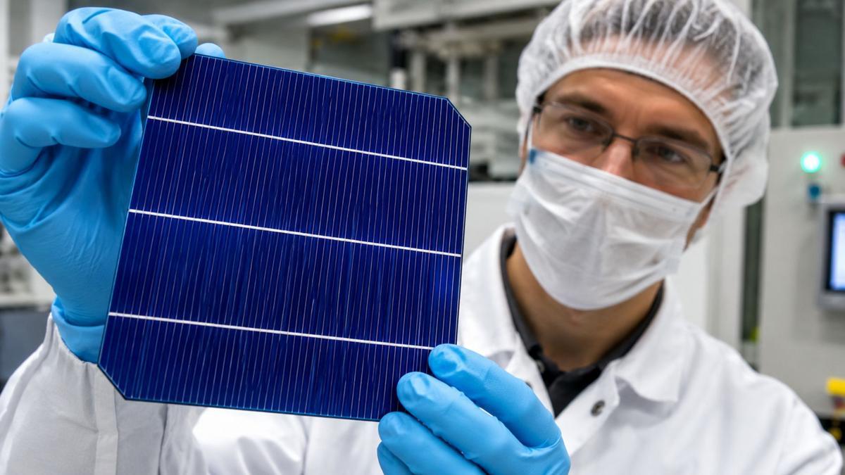
Joint study by USP and York University uses computational models to simulate nanostructures that mimic black silicon with reduced surface area.
The quest for higher solar energy conversion efficiency has taken a significant step in academia.
A recent study shows that optical properties similar to traditional black silicon can be simulated using microscopic structures that cover less than half the surface area typically used in industry research.
This breakthrough results from a scientific collaboration between researchers from the University of São Paulo (USP) and the British University of York.
Published in the specialized journal IEEE Journal of Photovoltaics, the work examines how specific nanometer-scale geometries can handle sunlight without the need for extensive textures.
The Challenge of Light and Electrical Charges
The term black silicon derives from the dark appearance the material takes when subjected to texturing treatments.
This physical change primarily aims to minimize light reflection, allowing a much larger portion of solar radiation to penetrate the structure instead of being reflected back into the environment.
However, attracting more radiation is only the first step in the photovoltaic energy generation process.
Within a solar cell, the captured light must be efficiently converted into electrical charges, a flow that can encounter barriers when the surface has excessive irregularities, leading to unwanted electron recombination.
To overcome this technical hurdle, the team focused on evaluating alternative geometries through advanced computational simulations.
The tests examined conical textures with dimensions comparable to light wavelengths, seeking the ideal balance between light capture and preservation of the material’s electrical properties.
The simulations assessed conical structures capable of exhibiting anti-reflective properties similar to those attributed to black silicon, but with less than half the surface area of some reference configurations.
Optimized Geometry Without Raw Material Reduction
It is essential to emphasize that the concept of surface area, in this specific context, refers exclusively to the extent of the exposed and textured surface, not to the total silicon consumption or the raw material mass required to manufacture a panel.
Therefore, the scientists stress that the model does not translate into a direct savings of industrial inputs or a reduction in manufacturing costs.
The main gain lies in the mathematical modeling, which points to promising avenues for future experimental investigations.
Avoiding overly complex surfaces can mitigate issues in the behavior of electric charges, preserving the overall performance of the semiconductor device without sacrificing the anti‑reflection effect.
Perspectives and Next Steps
Despite the enthusiasm generated by the computational data, the authors note that the study does not present a commercial device ready for large‑scale deployment, nor does it demonstrate an immediate gain in electrical efficiency for real photovoltaic cells.
The calculated optical behavior must be empirically validated in the laboratory.
The transition from the virtual environment to industry will require complex nanofabrication steps, rigorous dimensional control, and testing with complete solar cells.
The central contribution of the project lies in opening new routes for technological development, reconciling optimized light capture with the structural integrity required for future solar panels.